The pin names of the BTT Scylla V1 in the firmware
BTT Scylla V1 Pinout Diagram
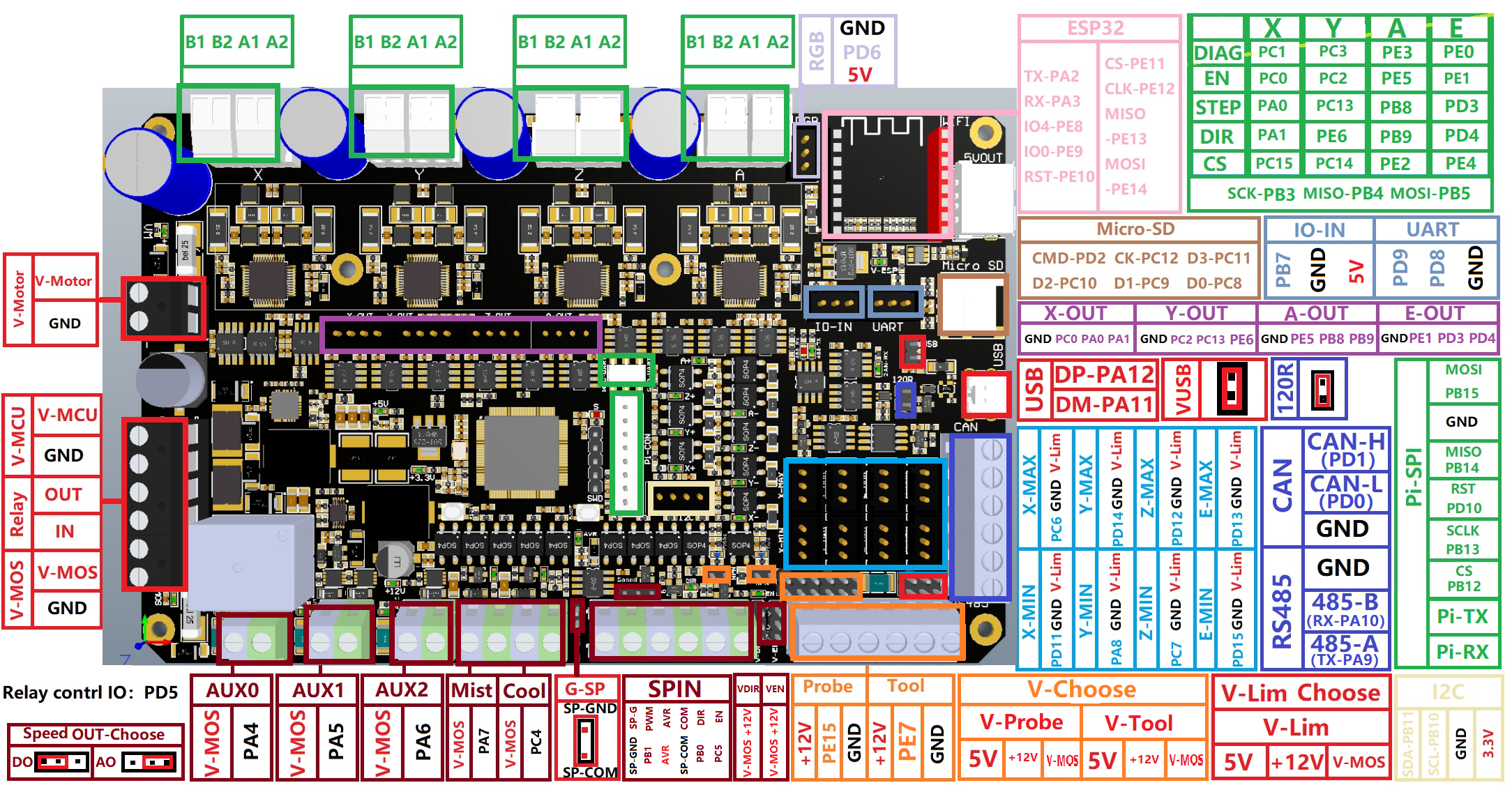
BTT Scylla V1 Driver Pins in Firmware
Driver pin numbers. They are separated into driver number.
| Pin Type | 0 | 1 | 2 | 3 |
|---|---|---|---|---|
| Enable Pins | PC_0 | PC_2 | PE_5 | PE_1 |
| Step Pins | PA_0 | PC_13 | PB_8 | PD_3 |
| Direction Pins | PA_1 | PE_6 | PB_9 | PD_4 |
| UART Pins | PC_15 | PC_14 | PE_2 | PE_4 |
BTT Scylla V1 Other Pins in Firmware
If more than one pin name is availble, either name can be used in the firmware (config.g).
If the pins aren’t in the table (due to not having a special name), then the pin itself can be used in the form of PA0, PA.0, PA_0, A0, A.0 or A_0.
| Pin | Pin Name(s) | PWM Timer (up to 3.6) | PWM Timer (from 3.7) |
|---|---|---|---|
| PA_4 | aux0pwm, aux0 | ||
| PA_5 | aux1pwm, aux1 | Timer 2 | Timer 2 |
| PA_6 | aux2pwm, aux2 | Timer 13 | Timer 13 |
| PA_7 | mistpwm, mist | Timer 14 | Timer 14 |
| PA_8 | ymin | ||
| PA_9 | tx1, rs485a | ||
| PA_10 | rx1, rs485b | ||
| PB_0 | spindledir | Timer 3 | Timer 8 |
| PB_1 | spindlepwm | Timer 3 | Timer 8 |
| PB_7 | extin0, ioin | Timer 4 | Timer 4 |
| PB_10 | scl | Timer 2 | Timer 2 |
| PB_11 | sda | Timer 2 | Timer 2 |
| PC_1 | xdiag | ||
| PC_3 | ydiag | ||
| PC_4 | coolantpwm, coolant, cool | ||
| PC_5 | spindleen | ||
| PC_6 | xmax | Timer 3 | Timer 8 |
| PC_7 | zmin | Timer 8 | Timer 8 |
| PD_5 | relayctr, relay | ||
| PD_6 | rgbpwm, neopixel | ||
| PD_8 | tx3 | ||
| PD_9 | rx3 | ||
| PD_11 | xmin | ||
| PD_12 | zmax | Timer 4 | Timer 4 |
| PD_13 | amax | Timer 4 | Timer 4 |
| PD_14 | ymax | Timer 4 | Timer 4 |
| PD_15 | amin | Timer 4 | Timer 4 |
| PE_0 | adiag | ||
| PE_3 | zdiag | ||
| PE_7 | tool | ||
| PE_15 | probe |
BTT Scylla V1 Configured SPI connections
The below SPI channels are preconfigured in the firmware.
Where NoPin is present, then that pin is not configured by default.
| SPI Channel | CLK | MISO | MOSI | Hardware or Software | Use |
|---|---|---|---|---|---|
| 0 | NoPin | NoPin | NoPin | Hardware | None |
| 1 | PB_13 | PB_14 | PB_15 | Hardware | SBC SPI |
| 2 | PB_3 | PB_4 | PB_5 | Hardware | Drivers |
| 3 | NoPin | NoPin | NoPin | Software | None |
| 4 | PB_3 | PB_4 | PB_5 | Software | None |
| 5 | NoPin | NoPin | NoPin | Software | None |
| 6 | PE_12 | PE_13 | PE_14 | Hardware | WiFi |
| 7 | NoPin | NoPin | NoPin | Hardware | None |
| 8 | NoPin | NoPin | NoPin | Hardware | None |